Prof. Dmitri Donetski: Infrared Imaging, LIDAR and X-ray Beam Position Monitoring for Synchrotron Light Sources
 |
| Professor Dmitri Donetski |
Dmitri’s interests revolve around the development of novel semiconductors structures for quantum photon detection and integrated systems for remote sensing and imaging. Spectral responses of designed sensors vary from long wave infrared (LWIR) to soft x-ray ranges. These III-V compound semiconductor structures are grown in-house by Gela Kipshidze with the Molecular Beam Epitaxy (MBE) system maintained by the Optoelectronics Group. Semiconductor wafers are processed into devices and tested by students. The research is performed in three directions: photon detectors for imaging in LWIR, beam steering devices for LIDAR (optical radar) and photodetector arrays for soft X-ray beam position monitoring.
Details of each follow below.
1. Quantum detectors for LWIR imaging
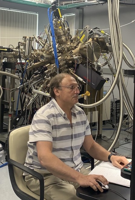 |
| Stony Brook Molecular Beam Expitaxy System with Gela Kipshidze |
Most information is obtained by imaging. Imaging in LWIR range (photon energies < 0.1 eV) allows for capture of thermal emission of objects in complete darkness, and can reveal minor temperature differences on object surfaces. LWIR radiation can pass through fog, smoke, and dust due to reduced light scattering. It is used for studying climate changes. LWIR imaging can be used in medical diagnostics, such as identifying inflammation, tumors, or irregularities in blood flow.
For high contrast low noise imaging in the long wave infrared range, the sensors should possess the greatest quantum efficiency – delivering the highest photocurrent for a given number of photons. The sensor heterostructures are being grown in-house by the Optoelectronics Group’s MBE system and processed into detectors of various dimensions for measurement of device benchmark parameters. These heterostructures utilize the InAsSb sensing region with lattice constants greater than that of GaSb substrate which removes constraints present in competing designs.
It should be noted that InAsSb is a semiconductor material created by alloying InAs and InSb compounds (where In is Indium, As is arsenic and Sb is Antimony). The development of technology for the growth of high-quality InAsSb compounds with elevated lattice constants in Stony Brook resulted in a pleasant discovery that these materials exhibit much lower energy gaps compared to what was commonly believed possible for many years and can be used for sensing applications in the long wave infrared range. The novel approach enables the use of InAsSb absorbers with large Sb compositions which results in 2-3 fold greater absorption and an order of magnitude greater carrier mobility necessary for the realization of sensors with high quantum efficiency. The project involved two students, Jingze Zhao currently working toward his PhD and Jinghe Liu who recently graduated and now works at Apple. The project is sponsored by the Center for Semiconductor Modeling at the Boston University, the Army Research Laboratory, and industry.
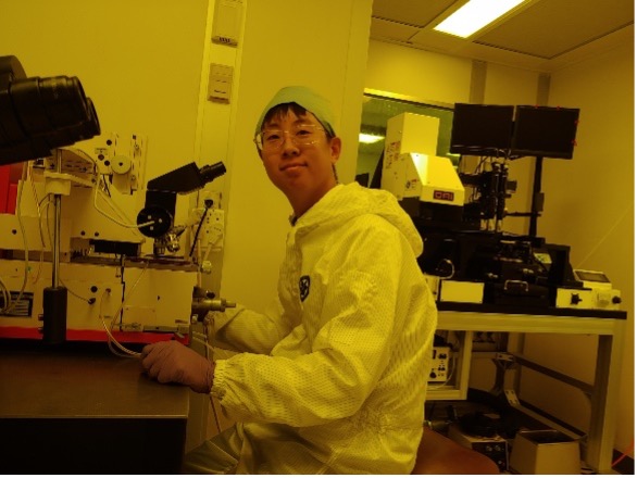
Jingze Zhao is performing mask alignment in processing the InAsSb-based heterostructures grown in house by MBE into long-wave infrared sensors for research toward his PhD degree.
2. LIDAR
Navigation systems of autonomous vehicles rely on fast and accurate determination of distances to objects and object shapes, made possible by mapping scenes with a pulsed laser also known as Light Detection and Ranging (LiDAR). Applications of LWIR lasers make LIDAR operation less dependent on poor weather conditions. In many applications, the use of moving mirrors for laser beam steering is not sufficiently fast and reliable. Electrical control of the refractive index of long-wave infrared materials with the use of the electro-optical effect required high voltage high power drivers operating on a load with reactive impedance limiting the electrical bandwidth due to challenging impedance matching.
It was recently shown however that InAsSb alloys grown by the MBE system can be used for electrical control of the refractive index of the materials in mid-wave and long-wave infrared ranges with bandwidths of tens of MHz with low voltages and currents compatible with CMOS electronic circuits. This makes possible electronic beam steering. The devices can be designed with an active impedance for broadband impedance matching and integration of the beam steering devices with driver electronics into a compact system. The project is sponsored by the Army Research Office.
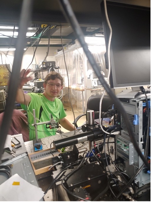
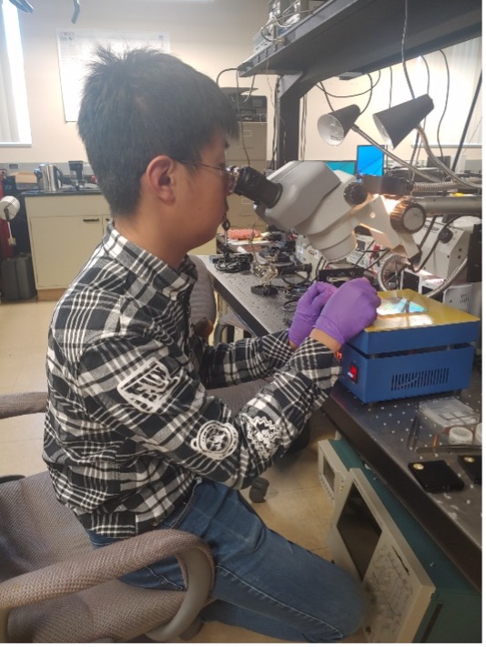
Kevin Kucharczyk is measuring the GaAs photodiode responsivity (left). Jingze Zhao is mounting InAsSb detectors (right).
3. Synchrotron X-ray beam position monitoring
Imaging with coherent soft X-rays (photon energies up to 2 keV) is essential to advance our understanding of the laws of nature, material, and biological research. It is performed by mapping the light scattered by an object with a scanning CCD camera over a period of several hours followed by image reconstruction. The fundamental resolution limit for coherent soft X-ray imaging is due to the finite stability of electron and photon beams in synchrotron light sources. Getting artifact-free images requires monitoring and maintaining photon beam positional stability down to micron-level accuracy.
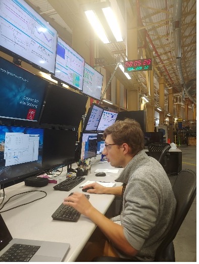 |
| Kevin Kucharczyk is collecting the data on responsivity the semiconductor sensors fabricated at Stony Brook and installed at the Coherent Soft Xray beamline CSX23 at the NSLS-II. |
The commonly employed X-ray beam position monitors for hard X-ray range are based on photoemission from metals. In the soft X-ray range, this approach is not acceptable for coherent beamlines due to a drop of photoemission in the soft X-ray range which requires a deeper penetration of the metal blades used in the traditional approach into the beam. The latter results in unwanted wavefront distortion so that non-invasive in-situ beam position monitors for coherent soft X-rays virtually do not exist.
In this project conducted at the National Synchrotron Light Source NSLS-II at Brookhaven National Laboratory, we proposed to use semiconductor arrays of photodiodes placed in a halo of the X-ray beam. The internal photo-effect in semiconductors results in the generation of a much larger number of hole pairs compared to photoemission in metals which offers superior responsivity and response linearity of semiconductors sensors in the soft X-ray range and reconstruction of the beam center position by measurements of the beam intensity in a halo without disturbing the beam wavefront distortion and coherency. The project is sponsored by the US Department of Energy Brookhaven National Laboratory.
Teacher and Scholar
Dmitri Donetski is with Stony Brook University since 1996. He is currently teaching ESE118 Digital Logic Design and ESE411 Analog Integrated Circuits in the Fall and Spring semesters, respectively. Similar courses, EEO218, EEO219, and EEO311 are offered online.
